
- Home > News > Industry News
Application of UV Lasers in Precision Machining of Brittle Materials
2025-09-09Laser manufacturing technology utilizes the physical interaction between a high-energy laser beam and a material, achieving precision processing by vaporizing, ablating, or modifying the material's properties through concentrated energy release. In recent years, this technology has rapidly penetrated various fields of industrial manufacturing, particularly dominating materials processing.
Data shows that laser processing of metals now accounts for over 80% of the overall market, making it the technology's core application. Metals are a prime candidate for laser processing primarily because iron, copper, aluminum, and their alloys are typically high-hardness metals with excellent laser absorption and response characteristics, enabling efficient melting, cutting, or welding. These materials couple effectively with the laser beam, resulting in a stable processing process and high-quality results. In many common applications, such as laser cutting or basic welding of sheet metal, operators typically only need to adjust the laser output power to achieve the desired result. These applications require relatively low-level control of process parameters and offer a low technical barrier to entry. This is why laser processing has rapidly gained popularity and widespread adoption in the manufacturing industry.
However, in daily life and high-end manufacturing, a large number of non-metallic materials are used, such as flexible materials, thermoplastics, heat-sensitive materials, ceramics, semiconductors, and brittle materials such as glass. These materials place higher demands on process accuracy when undergoing laser processing - not only do they need to precisely control the beam characteristics and energy distribution, but they also need to strictly manage the ablation depth and thermal damage area of the material to avoid cracking, deformation, or performance degradation. Especially in scenarios where ultra-fine processing is pursued, it is often necessary to achieve processing accuracy at the micron or even nanometer level. Traditional commonly used infrared lasers are difficult to meet such high-precision requirements due to their large thermal impact and limited focusing limits. In contrast, ultraviolet lasers, with their short wavelength, high photon energy, and extremely small heat-affected zone, can achieve a "cold processing" effect. They are particularly suitable for precision cutting, drilling, or surface modification of such sensitive, fragile, or high-precision non-metallic materials, making them an ideal choice for such applications.
Main Types and Applications of UV Lasers
Ultraviolet lasers refer to invisible light with a wavelength in the ultraviolet range that is imperceptible to the human eye. In industrial processing, mainstream UV lasers are currently divided into two main categories: solid-state UV lasers and gas UV lasers.
Solid-state UV lasers are typically obtained by frequency tripling an infrared-band all-solid-state laser, with an output wavelength typically around 355 nm. Recent technological advances in these lasers have enabled pulse widths to leap from nanoseconds to picoseconds and even shorter, significantly improving processing precision and reducing thermal effects.
Gas-type UV lasers, represented by excimer lasers, have an output wavelength that covers the deep ultraviolet range and are widely used in high-precision applications such as ophthalmic refractive surgery, semiconductor lithography, and micro-patterning. Meanwhile, with continuous breakthroughs in fiber laser technology, fiber lasers in the UV range are gradually entering the market. Picosecond UV fiber lasers, in particular, are becoming a new force in ultra-fine processing due to their excellent stability, high beam quality, and ease of maintenance.
However, due to the large energy loss and heat accumulation during the frequency doubling conversion process of ultraviolet lasers, the overall photoelectric conversion efficiency is low and the manufacturing cost remains high. Therefore, there is still a technical bottleneck in the pursuit of higher average power output. Despite this, due to its short wavelength and high single-photon energy characteristics, ultraviolet lasers mainly act on materials through "photochemical ablation" with minimal thermal impact, and are therefore often called "cold light sources." This "cold processing" mechanism enables it to perform well in the precision processing of brittle or heat-sensitive materials such as glass, ceramics, and polymers, making it an indispensable key technology in micro-nano manufacturing and high-end electronics manufacturing.
UV Laser Processing for Common Brittle Materials
1. Glass
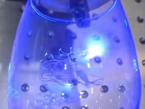
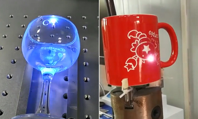
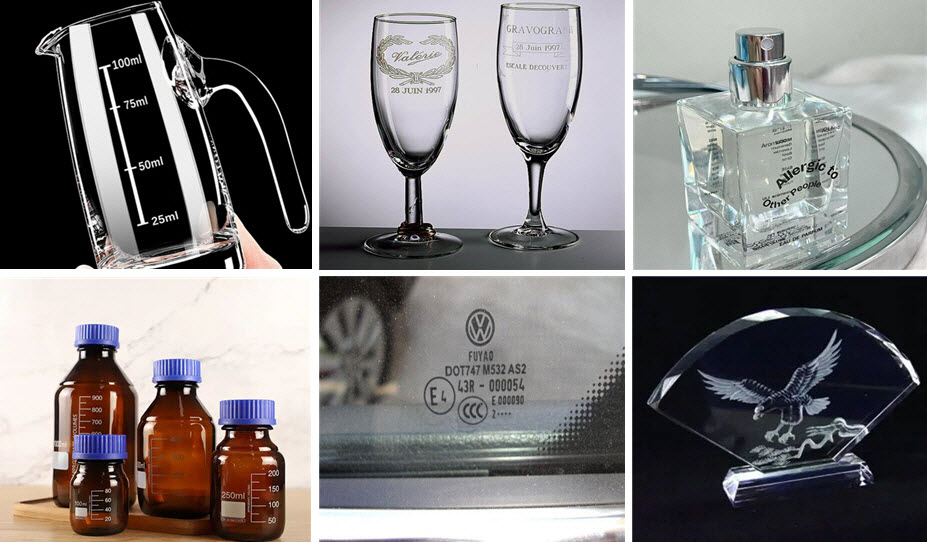
Glass is a material widely used in everyday life, often found in drinking glasses, wine glasses, storage containers, and various decorative crafts. Engraving or marking patterns on glass surfaces has long faced numerous challenges. Traditional processing methods such as sandblasting, silk screen printing, or mechanical scribing often lead to high cracking and breakage rates due to stress concentration, and are difficult to achieve intricate patterns. They can also be associated with environmental pollution and insufficient processing precision.
The emergence of UV laser technology has provided an ideal solution for glass surface processing. With its short wavelength and high photon energy, UV lasers can act directly on the glass surface in a "cold processing" manner, modifying or micro-etching the material through a photochemical effect, thereby completing marking and patterning. This process minimizes thermal impact, preventing heat-induced cracking or edge chipping on the glass. It also enables micron-level engraving, resulting in clear, detailed, and permanent images and text. Therefore, UV laser marking not only overcomes the drawbacks of traditional processes such as low precision, poor yield, and high pollution, but also significantly enhances design freedom and production efficiency. Today, it is widely used in industries such as wineware, glassware, and craft gifts, becoming an indispensable core technology for personalized customization and high-end surface decoration. It is hailed as a revolutionary force in the field of glass deep processing.
2. Ceramics
Ceramic materials are not only widely used in architectural tiles, household utensils, and decorative crafts, but also play an increasingly important role in modern electronic technology. For example, several mobile phone manufacturers have launched flagship models with high-performance ceramic back covers, which have gained market attention for their excellent texture and wear resistance. Furthermore, in the mobile communications, optical communications, and consumer electronics fields, precision components such as ceramic ferrules, ceramic substrates, package bases, and ceramic covers for fingerprint recognition modules are widely used.
As electronic devices move towards miniaturization and high integration, the requirements for processing precision and surface quality of ceramic components are also increasing. Traditional mechanical processing methods are prone to edge chipping, micro-cracks, or require subsequent polishing, making them unable to meet high-end requirements. In contrast, UV laser cutting technology, thanks to its "cold working" properties, is currently an ideal solution for processing thin ceramic wafers. Its short-wavelength laser enables high-precision cutting at the micron level, with a minimal heat-affected zone, effectively eliminating the risk of thermal stress-induced fractures. The cut edges are smooth, and the finished product is formed in one go, eliminating the need for secondary processing.
Precisely due to these advantages, the application of UV lasers in precision ceramic processing is rapidly expanding. In the future, it will play a key role in more high-end electronics manufacturing fields, driving the profound transformation of ceramic materials from traditional industries to high-tech ones.
3. Wafer Cutting
In the semiconductor and optoelectronics industries, sapphire substrates are widely used in the manufacture of devices such as blue and white LEDs due to their excellent physical and chemical stability. However, their extreme hardness presents significant challenges to traditional wheel cutting methods: not only are tools subject to severe wear and high processing costs, but the cut line widths often exceed 30μm, resulting in reduced wafer utilization, a reduced chip count, and a low overall yield rate. With the rapid development of the LED industry, the market is placing higher demands on the efficiency, precision, and yield of sapphire wafer cutting.
UV laser cutting technology offers a highly effective solution. Leveraging its high focusing precision and "cold working" properties, UV lasers can achieve micron-level narrow kerfs, significantly improving material utilization. The cutting process minimizes thermal impact, effectively avoiding cracks and edge chipping, resulting in smooth, flat cuts and significantly improving chip yield and reliability. Furthermore, the non-contact processing method reduces mechanical stress and tool wear, making it a mainstream technology in sapphire wafer processing.
4. Quartz Cutting
Furthermore, quartz, due to its high brittleness and low toughness, has long been considered a challenge in industrial processing. Traditional methods rely primarily on diamond grinding wheels and saw blades for "hard-on-hard" cutting, which not only results in high consumables costs, but also easily causes edge damage and makes it difficult to control processing precision. UV lasers, with their positioning accuracy of up to ±0.02mm, have revolutionized quartz cutting. By precisely controlling laser power and scanning path, smooth, clean cut surfaces can be achieved without causing material fracture, and cutting speeds far exceed those of traditional manual or mechanical methods. The entire process is fully digitally controlled by a computer, with parameters adjustable and monitored in real time. The intuitive user interface significantly lowers the barrier to entry and improves production consistency and automation. Consequently, UV lasers are gradually replacing traditional processes and becoming the ideal choice for high-precision quartz processing.
Due to its "cold processing" properties, UV lasers are considered a key technology in laser precision manufacturing. They exhibit unique advantages in fabricating micron- and even nanoscale structures, making them an ideal choice for high-precision applications. However, their widespread adoption has been hampered by multiple technical bottlenecks: the complex frequency-doubled conversion process, poor equipment stability, high manufacturing costs, and thermal management challenges, making output power difficult to increase. This has limited their use to niche, high-end applications. In recent years, continuous breakthroughs in core optical components, heat dissipation design, and laser architecture have significantly increased UV laser power output, while production costs have gradually decreased, significantly improving their cost-effectiveness and driving their rapid adoption. The past three years have seen explosive growth in market applications, with product forms also becoming increasingly diverse. In addition to traditional nanosecond UV lasers, higher-performing picosecond UV lasers and fiber-based ultrafast UV lasers have matured and entered the market. These technological advances not only improve processing accuracy and efficiency, but also further broaden the application boundaries of ultraviolet lasers in cutting-edge fields such as semiconductors, displays, biomedicine, and precision electronics, enabling them to gradually move from "high-threshold technology" to large-scale industrial applications.